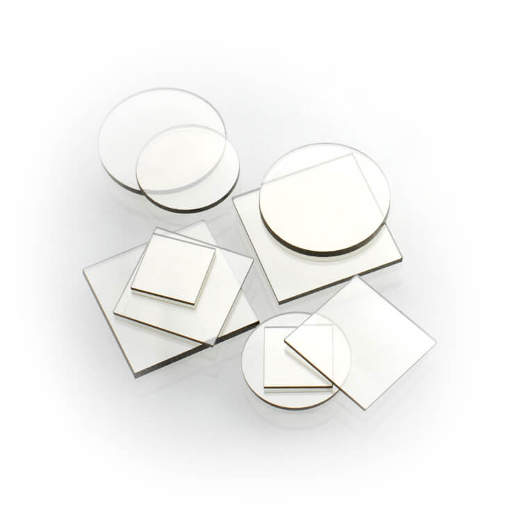
ELECTRICAL GRADE
Due to the promising outcomes demonstrated by CVD diamonds, there are several applications of diamonds in the products like RF diodes, BJT, MOSFET, MEMS, etc. in the electronic sector. Diamonds with specific characteristics may now be produced for radiation detection due to remarkable advancements in CVD diamond production. Exciting future developments and huge area homo-epitaxial generated single crystal diamond plates/films are possible because to ongoing progress in CVD techniques.

Size: 2.0x2.0mm
Thickness: 0.50mm
Carat Weight EA : 0.03 ct
Price : $655

Size: 3.0x3.0mm
Thickness: 0.50mm
Carat Weight EA : 0.08 ct
Price : $1450

Size: 4.5x4.5mm
Thickness: 0.50mm
Carat Weight EA : 0.17 ct
Price : $2150

Size: 2.0x2.0mm
Thickness: 0.30mm
Carat Weight EA : 0.02 ct
Price : $750

Size: 3.0x3.0mm
Thickness: 0.30mm
Carat Weight EA : 0.05 ct
Price : $1625

Size: 4.5x4.5mm
Thickness: 0.30mm
Carat Weight EA : 0.1 ct
Price : $2480